Application laboratory time-resolved cathodoluminescence spectroscopy (ZALKAL)
German: Applikationslabor Zeitaufgelöste Kathodolumineszenzspektroskopie (ZALKAL)
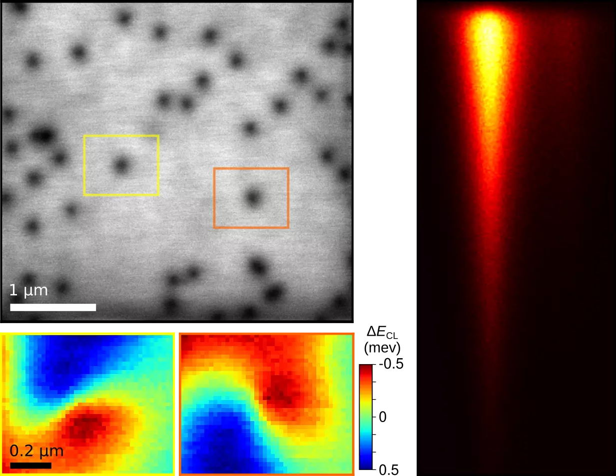
Paul Drude Institute has 30 years of experience in the field of cathodoluminescence (CL) spectroscopy, which analyzes the light emitted by semiconductors under electron irradiation. The light is emitted when charge carriers (electrons and holes) recombine and its wavelength is determined, among other things, by the band gap of the semiconductor. Based on a scanning electron microscope (SEM), this offers the possibility to investigate properties of semiconductor structures with extremely high spatial and spectral resolution. On the one hand, this allows a more detailed understanding of structural defects in the crystal structure as they influence the light emission and thus their influence on desired properties can be investigated. On the other hand, nanoscopic structures can be investigated that have been incorporated into the semiconductor to tailor its functionality. However, knowledge on the dynamics, i.e. the temporal behavior of the charge carriers, which cannot be investigated with a classical CL system, are crucial for a comprehensive understanding of where charge carriers are lost, i.e. efficiency is lost in the structures. The required high temporal resolution is achieved by pulsing the electron beam on a picosecond timescale combined with ultrafast detectors.
PDI is currently building up an application laboratory for time-resolved cathodoluminescence spectroscopy, where the detectors will be optimized for ultraviolet wavelengths down to about 180 nm. However, the visible and near-infrared spectral regions will be covered as well, thus covering a wide range of materials. The system will be capable of measuring classic semiconductor thin-films and heterostructures, 2D materials, as well as 3D nanostructures. It thus can contribute to a wide range of the research activities at PDI. However, we will also closely collaborate with other research institutes and academic partners working on semiconductors in Berlin and beyond, as well as companies that require the combination of spectral and time-resolved luminescence mapping. Using the existing infrastructure of the analytical SEM lab, measurements can be correlated to maps of the composition (energy-dispersive x-ray spectroscopy, EDX), crystal structure (electron backscatter detection, EBSD) and charge collection (electron beam induced current, EBIC).

The application lab is co-funded by the European Regional Development Fund through the Berlin State Government (Senate) from January 2023 through December 2025.