PDI confirms existence of Bi_Ga hetero-antisites in landmark study
/ Announcements , News
An invited paper by PDI Senior Scientist Esperanza Luna Garcia de la Infanta was recently selected as Featured article (Journal Editors’ choice) in a special issue of the Journal of Applied Physics, “Native Defects, Impurities and the Electronic Structure of Compound Semiconductors: A Tribute to Dr. Wladyslaw Walukiewicz”. Dr. Walukiewicz (1946–2022) contributed to semiconductor physics with studies on the relationships between defects, dopant impurities, the electronic structure of semiconductors, and their resulting optical and transport properties, among others. The study is part of an ongoing collaboration between PDI and researchers from Tampere University, Finland.
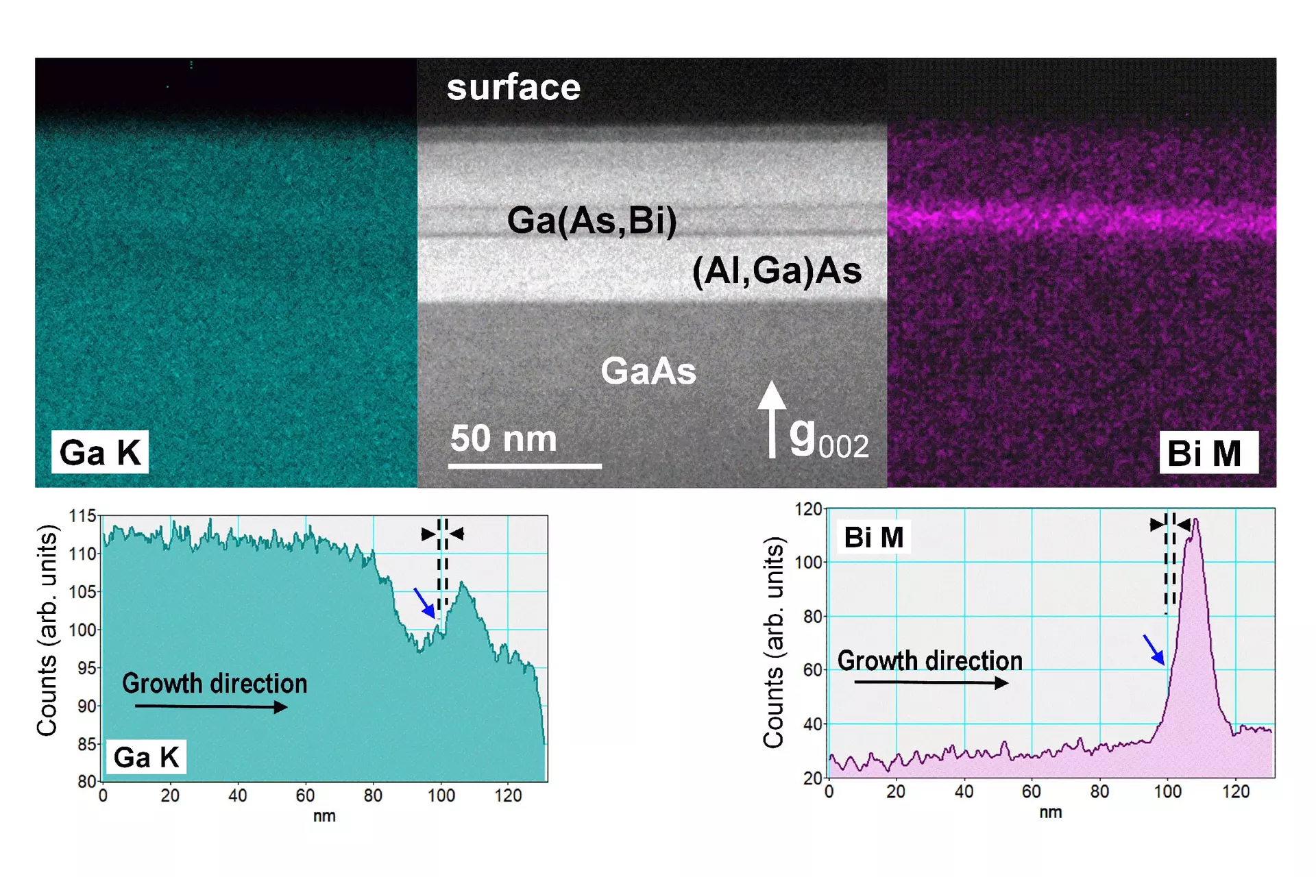
The paper reports on the detection of BiGa hetero-antisites, a highly anticipated yet challenging to detect defect in dilute bismides at the interfaces of Ga(As,Bi)/(Al,Ga)As quantum well structures grown by molecular beam epitaxy (MBE).
The research conducted at PDI marks the second-ever published experimental confirmation of BiGa hetero-antisites, where bismuth (Bi) is incorporated at the group-III atom position. This discovery significantly advances the ability to identify point defects in Ga(As,Bi), a crucial step in enhancing material quality and facilitating practical applications. The sole previous study on this topic was published three decades ago when BiGa hetero-antisites were detected in Bi-doped bulk GaAs using optical techniques. Subsequent efforts to detect these defects have been challenging, with many studies speculating on their existence in the innovative dilute-bismide alloy without concrete experimental proof. This paper presents the inaugural experimental evidence of BiGa hetero-antisites in layers grown via MBE. Furthermore, detection is made by employing diffraction-based g002 dark-field transmission electron microscopy (DFTEM). The spatial resolution associated with TEM enables the precise locatation of the defects, in this case at the interfaces of Ga(As,Bi)/(Al,Ga)As QW.
Whereas routine scanning (S)TEM may overlook any anomaly, this work demonstrates how chemically-sensitive g002 DFTEM imaging reveals unexpected features associated with the presence of these point defects with remarkable clarity. Specifically, the presence of BiGa hetero-antisites is vividly illustrated by distinct “dark-lines” at the interfaces. Additional analytical STEM procedures and revised STEM measurements specifically aimed to detect any anomaly at the interfaces reveal Ga depletion and Bi accumulation at the exact position of the dark-lines, consistent with BiGa at this location. The formation of BiGa hetero-antisites is discussed in the context of some specific procedures during MBE growth. This highlights the relevance of combined TEM and MBE investigations —an area in which PDI has pioneered and gained global recognition—in advancing materials science.
Dilute bismide alloys, such as Ga(As,Bi), represent a fascinating class of novel materials that have garnered significant attention due to their unique properties and potential applications in various fields. These alloys are derived from III-V semiconductors by incorporating a small percentage of bismuth (Bi) at the group-V atom position. The resulting materials exhibit intriguing properties such as a large reduction in the bandgap, large enhancement of the spin-orbit splitting, and an almost temperature-insensitive band gap dependence, making them promising candidates for high-efficiency solar cells, infrared optoelectronic devices, and spintronic applications. Despite their immense potential, the precise understanding of Bi incorporation into the lattice has remained challenging yet essential for optimizing material quality and harnessing their full functionality. The recent work reported at PDI, demonstrating the presence of BiGa hetero-antisites in Ga(As,Bi)/(Al,Ga)As quantum well structures, represents a significant advancement in the field, shedding light on crucial point defect-related aspects crucial for material design and application development.
This work underscores g002 DFTEM imaging as a potent tool not only for dilute bismide alloys but also for detecting point defects across materials with zinc-blende crystal structure, highlighting its broader utility in materials research.
Publication: Detection of BiGa hetero-antisites at Ga(As,Bi)/(Al,Ga)As interfaces
Authors: Esperanza Luna, Janne Puustinen, Joonas Hilska, Mircea Guina
Journal: Journal of Applied Physics
DOI: https://doi.org/10.1063/5.0195965